- 您现在的位置:买卖IC网 > Sheet目录538 > ZVN4525E6TC (Diodes Inc)MOSFET N-CHAN 250V SOT23-6
ZVN4525E6
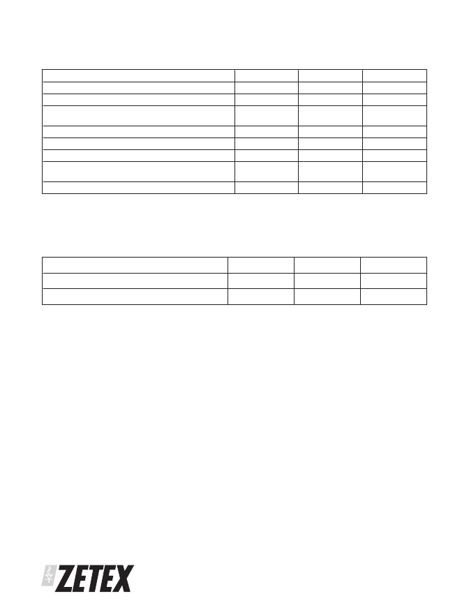
ABSOLUTE MAXIMUM RATINGS.
PARAMETER
Drain-Source Voltage
Gate Source Voltage
Continuous Drain Current (V GS =10V; TA=25°C)(a)
(V GS =10V; TA=70°C)(a)
Pulsed Drain Current (c)
Continuous Source Current (Body Diode)
Pulsed Source Current (Body Diode)
Power Dissipation at T A =25°C (a)
Linear Derating Factor
Operating and Storage Temperature Range
SYMBOL
V DSS
V GS
I D
I D
I DM
I S
I SM
P D
T j : T stg
LIMIT
250
± 40
230
183
1.44
1.1
1.44
1.1
8.8
-55 to +150
UNIT
V
V
mA
mA
A
A
A
W
mW/°C
°C
THERMAL RESISTANCE
PARAMETER
Junction to Ambient (a)
Junction to Ambient (b)
SYMBOL
R θ JA
R θ JA
VALUE
113
65
UNIT
°C/W
°C/W
NOTES
(a) For a device surface mounted on 25mm x 25mm FR4 PCB with high coverage of single sided 1oz copper,
in still air conditions
(b) For a device surface mounted on FR4 PCB measured at t 5 secs.
(c) Repetitive rating - pulse width limited by maximum junction temperature. Refer to Transient Thermal
NB High Voltage Applications
For high voltage applications, the appropriate industry sector guidelines should be considered with regard to
voltage spacing between conductors.
ISSUE 1 - MARCH 2001
2
发布紧急采购,3分钟左右您将得到回复。
相关PDF资料
ZVN4525GTC
MOSFET N-CHAN 250V SOT223
ZVN4525ZTA
MOSFET N-CH 250V 240MA SOT-89
ZVNL110ASTOB
MOSFET N-CHAN 100V TO92-3
ZVNL110GTC
MOSFET N-CHAN 100V SOT223
ZVNL120ASTZ
MOSFET N-CHAN 200V TO92-3
ZVNL120GTC
MOSFET N-CHAN 200V SOT223
ZVP0545ASTOB
MOSFET P-CHAN 450V TO92-3
ZVP0545GTC
MOSFET P-CHAN 450V SOT223
相关代理商/技术参数
ZVN4525G
制造商:ZETEX 制造商全称:ZETEX 功能描述:250V N-CHANNEL ENHANCEMENT MODE MOSFET
ZVN4525G(1)
制造商:ZETEX 制造商全称:ZETEX 功能描述:
ZVN4525GTA
功能描述:MOSFET N-Chnl 250V RoHS:否 制造商:STMicroelectronics 晶体管极性:N-Channel 汲极/源极击穿电压:650 V 闸/源击穿电压:25 V 漏极连续电流:130 A 电阻汲极/源极 RDS(导通):0.014 Ohms 配置:Single 最大工作温度: 安装风格:Through Hole 封装 / 箱体:Max247 封装:Tube
ZVN4525GTC
功能描述:MOSFET N-Chnl 250V RoHS:否 制造商:STMicroelectronics 晶体管极性:N-Channel 汲极/源极击穿电压:650 V 闸/源击穿电压:25 V 漏极连续电流:130 A 电阻汲极/源极 RDS(导通):0.014 Ohms 配置:Single 最大工作温度: 安装风格:Through Hole 封装 / 箱体:Max247 封装:Tube
ZVN4525Z
制造商:ZETEX 制造商全称:ZETEX 功能描述:250V N-CHANNEL ENHANCEMENT MODE MOSFET
ZVN4525Z(1)
制造商:ZETEX 制造商全称:ZETEX 功能描述:
ZVN4525ZTA
功能描述:MOSFET N-Chnl 250V RoHS:否 制造商:STMicroelectronics 晶体管极性:N-Channel 汲极/源极击穿电压:650 V 闸/源击穿电压:25 V 漏极连续电流:130 A 电阻汲极/源极 RDS(导通):0.014 Ohms 配置:Single 最大工作温度: 安装风格:Through Hole 封装 / 箱体:Max247 封装:Tube
ZVNA22
制造商:OMRON AUTOMATION AND SAFETY 功能描述:SWITCH ROLLER ARM LEVER SPDT 15A 制造商:OMRON INDUSTRIAL AUTOMATION 功能描述:Switch Limit N.O./N.C. SPDT Top Roller Arm Lever Conduit 15A 480VAC 250VDC 6.28N Linear Flange Mount
